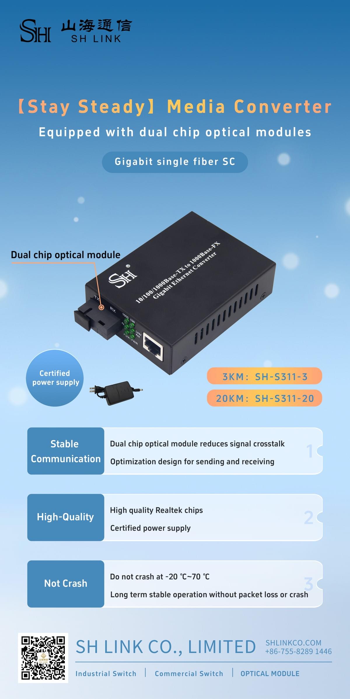
A common(4%-10%) issue with media converter operating in high temperatures is packet loss and system failure, which occurs due to malfunctions in the optical modules's chips under such conditions. Dual-chip 1*9 Optical Module was developed to SOLVE this problem!!! Keep your equipment work stably in high temperature.
In today’s rapidly evolving landscape of data centers, 5G transmission, and supercomputing networks, the stability and performance of optical modules directly determine the upper limits of communication system performance.
We promptly launched our groundbreaking dual-chip optical module, which shatters the performance limitations of traditional single-chip solutions with its revolutionary architecture, delivering core technological support for high-reliability, low- latency applications!
WHY Choose Dual-Chip?
1. Functional Partitioning and Architecture Design
Single-chip optical module:
Integrates the core functions of optical transmission(transmitter side) and optical reception(receiver side) --such as laser driving, modulation, photoelectric conversion, and signal amplification --onto a single chip, achieving functional division through internal circuitry.
l Advantages: Compact size, low power consumption, and reduced cost
l Disadvantages: High functional coupling, which may lead to performance degradation due to signal interference or thermal effects.
Dual-chip optical module
: Decouples the core functions of the transmitter and receiver into two dedicated chips(laser driver chip + receiver signal processing chip), enabling optimized performance for each subsystem.
l Advantage:Strong functional isolation, reducing signal crosstalk
l Disadvantage:Independent optimization for transmitter and receiver designs.
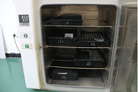
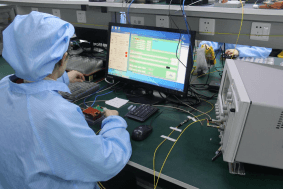
Aging test
2. Increased Performance Requirements
The dual-chip design enables more sophisticated chromatic dispersion compensation and signal equalization functions. While single-ship integration combines both transmitter and receiver functions--making signal processing susceptible to interference--the dual-chip solution allows independent optimization for each subsystem:
l Transmitter Side: Precise laser modulation control(e.g., EML lasers) to enhance signal purity.
l Receiver Side: Enhanced signal amplification and noise suppression(e.g., APD+TIA configuration) for improved sensitivity.
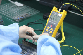
Optical Power Measurement
3. Signal Isolation and Anti-interference
Integrating transmitter (high-power laser driving) and receiver (high-sensitivity signal detection) circuits on a single chip increases susceptibility to electromagnetic interference-induced signal degradation. The dual-chip architecture mitigates crosstalk risks through physical isolation.
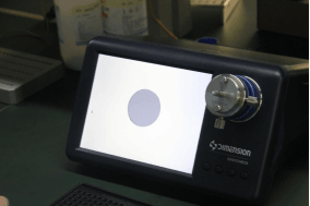
End-face Test
4. Thermal Management Optimization
Laser diodes generate significant heat, so designing a dedicated transmitter chip enables targeted thermal optimization, preventing heat-induced impacts on receiver-side circuits(e.g., temperature drift issues in transimpedance amplifiers).
Eye diagram
5. Reliability and Fault Isolation
Reducing single-point failure risks: By decoupling transmit and receive functions, if one chip fails, the other may remain operational(e.g., receiver failure won’t disrupt emergency transmissions from the transmitter).
Streamlined maintenance and testing: The dual-chip module allows independent performance testing of transmit or receive functions, significantly reducing production debugging complexity.
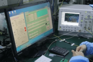
BER and Receiver Sensiticity Test
"Full Product Rortfolio Now Live!"
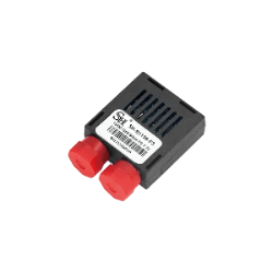
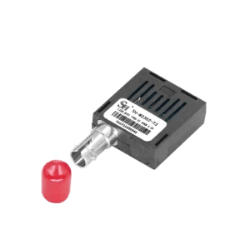
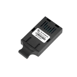
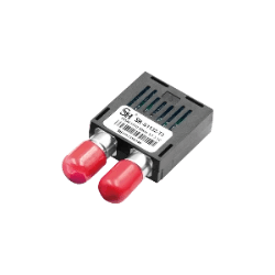
With deep expertise in 1*9 packaging technology, SH LINK comprehensive dual-chip optical module portfolio covers full rate options including 155Mbps, 622Mbps, and 1.25Gbps, supporting both single-mode and multi-mode transmission.
Offering SC, FC, and ST fiber optic interface options, our solutions are compatible with a wide range of communication equipment including optical terminals, fiber transceivers, fiber routers, CAN-to-fiber converters, switches, and UAV systems - meeting even the most demanding application requirements.
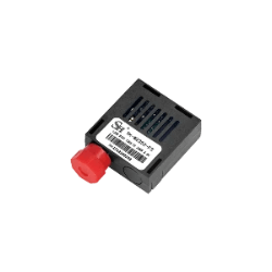
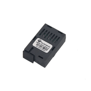
(P.S. “ Above: testing site photos. Below: product photos. ")